
A212 Electrical integration#
The A212 is a 60 GHz, multi-antenna radar system delivered as a one package solution with an integrated MCU, RF front-end and antennas (3TX, 4RX). To integrate it in your application, an external 26 MHz crystal, decoupling capacitors and power supply are required.
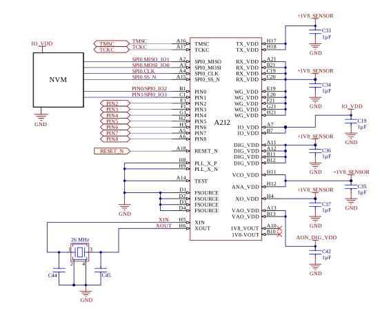
Some applications can run directly on the A212’s internal MCU, i.e. no external host is needed. For these cases an external NVM is required to boot the A212.
In production test the NVM can be flashed via the SPI (fastest), UART (slower) or the TCKC/TMSC pins (slowest).
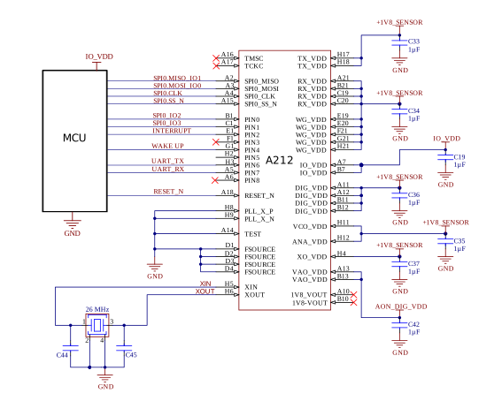
For applications that require an external MCU host, the NVM is optional since the sensor can boot from the external MCU. See Figure A: NVM integration and Figure B: MCU integration for example integrations.
Power#
A regulator is needed to provide 1.8V and IO_VDD to the sensor. IO_VDD supports both 3.3 V and 1.8 V. The total current consumption per sensor state is specified in the table Table 30 (Top = 25°C, nominal supplies):
Symbol |
Parameter |
Typ |
Unit |
Condition |
|---|---|---|---|---|
Isleep-ultra |
Current consumption, SLEEP-ULTRA-DEEP state |
40 |
µA |
|
Isleep-deep |
Current consumption, SLEEP-DEEP state |
46 |
µA |
|
Isleep-shallow |
Current consumption, SLEEP-SHALLOW state |
0.28 |
mA |
|
Iidle |
Current consumption, IDLE state |
1.1 |
mA |
|
Iprocessing |
Current consumption, PROCESSING state |
33 |
mA |
|
Imeasure |
Current consumption, MEASURE state |
174 |
mA |
Profile 1, 2, 3, 5; PRF = 27.7 MHz |
Imeasure-p6 |
Current consumption, MEASURE state |
182 |
mA |
Profile 6; PRF = 27.7 MHz |
Ifull |
Current consumption, FULL state |
192 |
mA |
Profile 1, 2, 3, 5; PRF = 27.7 MHz |
Ifull-p6 |
Current consumption, FULL state |
200 |
mA |
Profile 6; PRF = 27.7 MHz |
Supply noise#
Noise in the power supplies may affect the performance of the A212 sensor. Table 31 provides the recommended maximum ripple levels for the DIG_VDD, RX_VDD, TX_VDD, WG_VDD, XO_VDD, VCO_VDD and ANA_VDD supplies.
Frequency [kHz] |
Max supply ripple [mVpp] |
|---|---|
50 |
30 |
100 |
30 |
200 |
15 |
300 |
15 |
500 |
12 |
750 |
7 |
1000 |
7 |
1500 |
5 |
If the voltage source violates the supply ripple specifications in Table 31, an LC filter as shown in Figure 92 can be used. This filter has a cut-off frequency of 22 kHz. You can tune the values depending on the frequency and amplitude of the ripple. Be aware of the LC filter peaking at the series resonance frequency \(f_r = \frac{1}{2\pi\sqrt{LC}}\). A small snubber resistor (250 mΩ in the example) can be inserted to lower the Q factor.
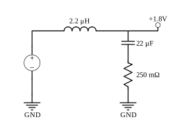
Figure 92 Optional LC supply filter.#
Crystal selection#
The A212 has a built in oscillator that requires an external 26 MHz crystal. The crystal connection diagram is shown in Figure 93.
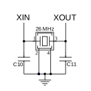
Figure 93 Crystal (XTAL) connection diagram.#
For the oscillator to be able to drive the crystal, the following criterion must be fulfilled:
where \(f_{xtal}\), \(C_L\) and \(R_{ESR}\) are defined in the crystal datasheet.
The load capacitance \(C_L\) is calculated as:
where:
\(C_{\text{parasitic}}\) is the PCB trace and package capacitance between the crystal pins (XIN and XOUT) and GND, expected to be between 1 pF and 2.5 pF per cm (depending on the trace width and stackup) plus package capacitance.
\(C_{10}\) and \(C_{11}\) can be calculated as:
Hardware schematics design checklist#
When designing the hardware schematics for the A212 sensor, the following checklist can be used to ensure a good design:
Does the selected crystal fulfill the load conditions according to the XTAL selection?
Are all ground pins of the A212 connected on the schematic symbol?
Does the selected regulator meets the Supply noise recommendations?
Are enable and interrupt pins connected?
Have you considered how to flash the NVM/MCU during production test?