
PCB guidelines#
As no RF components are required for the sensor integration, low-cost FR-4 type PCBs can generally be used. The following sections provide important information how to optimize the sensor PCB layout for good far-field directivity and side lobe level.
Component placement and routing#
The A121 sensor integrates folded dipole antennas, with the internal IC package ground plane extending beneath the entire sensor area serving as the primary ground reference. To further enhance directivity, the antenna ground plane should be extended onto the PCB by connecting all GND pads to the top copper layer. The PCB ground plane area adjacent to the sensor acts as a reflector and should therefore be a solid copper pour with minimal routing or external components. Two component placement options, shown in Figure 35 and Figure 36, are discussed in the following sections.
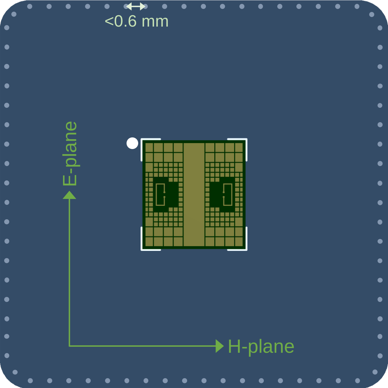
Figure 35 External components on sensor back side.# |
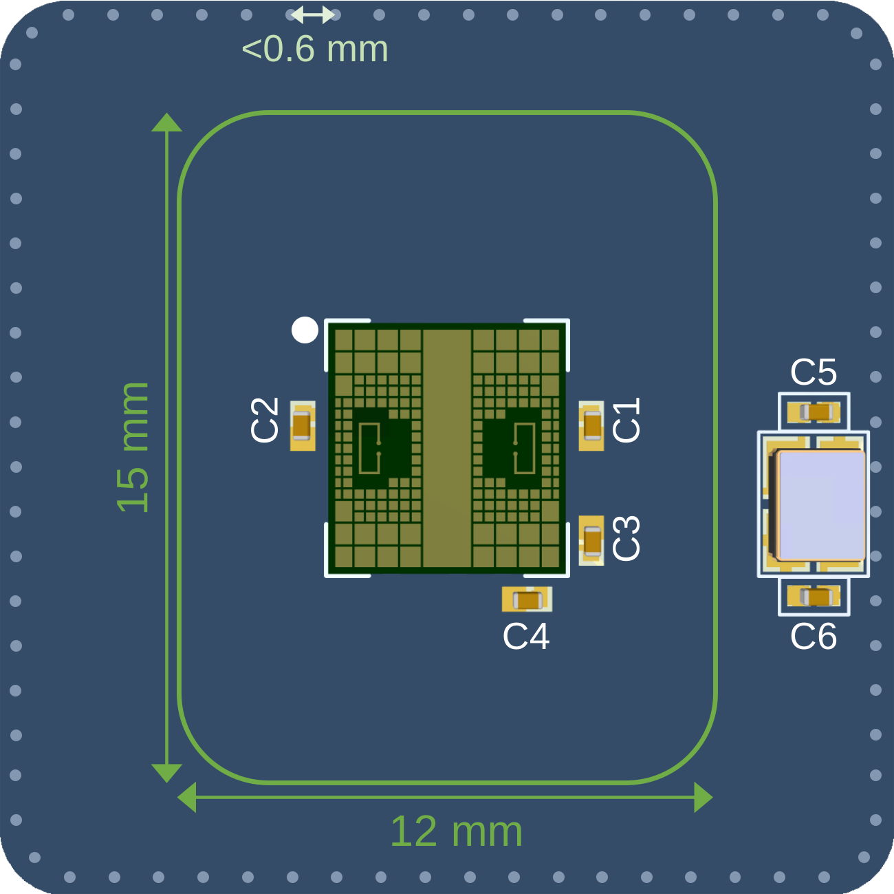
Figure 36 External components on sensor front side. Crystal is placed outside the marked clearance region (12x15 mm).# |
Components on sensor back side#
The preferred way is to place all external components such as decoupling capacitors and crystal on the opposite side of the sensor as this typically results in the highest directivity and lowest side lobe level (Figure 37). In addition, to maximize the radiated performance, consider the following:
Minimize the amount of routing on the sensor layer, at least within the clearance region in Figure 36. This can be done by routing the signals to the sensor with vias placed as close as possible to the sensor pads, see Figure 37. The ground plane area inside the footprint has lower impact on the radiated performance and therefore some vias and short traces are preferably placed there.
Whenever the assembly process allows, remove thermal reliefs on all sensor pads.
Choose small pad size vias such as 0.4-0.45 mm or smaller.
Minimize copper clearance for traces, vias, and pads on the sensor layer to maximize the ground plane area close to the sensor.
Add stitching vias with <0.6 mm spacing at the PCB outer edge to suppress potential edge radiation.
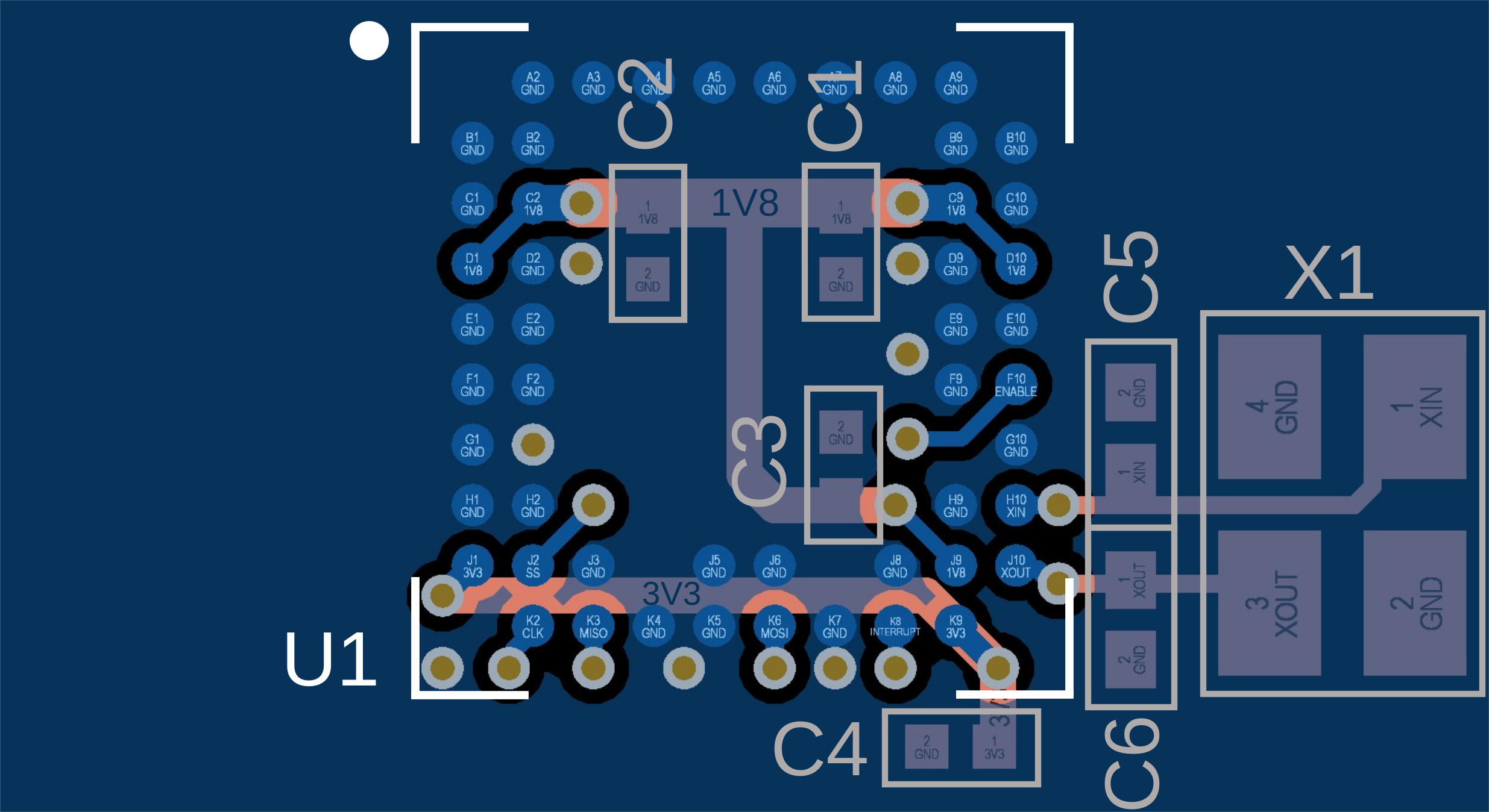
Figure 37 Layout example for 3.3 V I/O with sensor (U1) on top side and external components on back side. For 1.8 V I/O, C4 is optional.#
Components on sensor side#
External components can be placed on the same side as the sensor with negligible to small radiation pattern impact depending on placement and component size. To maximize the radiated performance in this case, consider the following aspects in addition to the aforementioned design rules
A121 decoupling capacitors can be placed adjacent to the sensor as in Figure 38. Choose smaller sized components such as metric 1005 (0402) or 0603 (0201).
Low-profile (< 1 mm) components such as the crystal, power management ICs and MCUs are placed outside the clearance region shown in Figure 36.
Larger components such as connectors, batteries, metallic screws and PCB standoffs can cause stronger radiation pattern distortion and when these need to be on the sensor side, they are best placed along the H-plane axis as far away as possible. Acconeer’s customer support can further help optimizing component placement for critical applications.
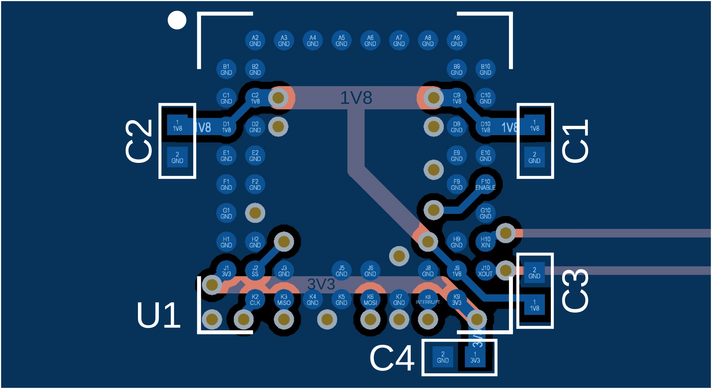
Figure 38 Layout example with external components on front side for 3.3 V I/O integration. For 1.8 V I/O, C4 is optional. Other components (e.g. crystal, MCUs) are preferably placed outside the clearance region in Figure 36.#
Ground plane size#
The normalized gain pattern for some different ground plane sizes are shown in Figure 39. As the ground plane size is increased, the directivity increases because of the larger reflector size. However, the directivity does not increase monotonically with ground plane size due to constructive and destructive interference. Also, see section Electromagnetic bandgap structures for side lobe suppression for implementing metasurfaces to further improve the side lobe level. For PCBs smaller than 15×15 mm, the H-plane side lobe level increases, which should be considered in applications where this is important.
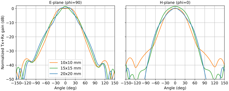
Figure 39 Normalized Tx+Rx gain for different ground plane sizes (simulated).#
Impact of conformal coating#
Conformal coating may be used to protect the sensor and other electronic components from environmental factors such as moisture, dust, and chemicals. Common conformal coatings are polymeric materials and we can therefore assume a relative permittivity \(\varepsilon_r\) between 2-4. Adding a coating layer on top of the sensor can impact the radiation patterns due multiple effects such as:
Offset in antenna resonance frequency as the antenna becomes electrically larger.
Reflection and refraction loss due to the interface between the sensor and the coating.
Dielectric loss in the coating material. This can usually be neglected for coating layers (e.g. < 200 µm).
Figure 40 shows the simulated gain pattern impact after a linear lossless (tan(δ)=0) coating has been added on top of the radar sensor and the PCB. For increasing coating thicknesses, the boresight gain decreases and the E-plane side lobe level increases. For critical applications where maximum boresight gain and low SLL is needed, it is recommended to use a thin coating layer (< 50 µm) with a low rel. permittivity and loss factor. As many coating materials are not well characterized at mmWave frequencies, performance should be verified with actual tests. Note that if the coating is only applied on the PCB, the impact will be significantly less.
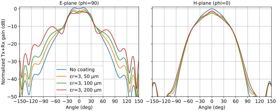
Figure 40 Simulated Tx+Rx gain impact of conformal coating for \(\varepsilon_r\) = 3.#
PCB design checklist#
When designing the PCB for the A121 sensor, the following checklist can be used to ensure a good design:
Have you connected all ground balls on the package?
Have you considered removing thermal reliefs on all ground pads to maximize directivity?
Did you place decoupling capacitors and other external components according to the guidelines under section Components on sensor back side?
Is the power supply and SPI interface routed with an adjacent ground plane?
Have you placed nearby ground vias to your signal and power supply vias?
Do you have stitching vias with <0.6 mm spacing at the PCB outer edge to suppress PCB edge radiation?
Have you considered adding EBGs for side lobe suppression?