
Electromagnetic bandgap structures for side lobe suppression#
The radiation pattern can be degraded by sidelobes, which represent unintentional sensitivity to directions outside the main beam. In fact, a reflection from a sidelobe direction can produce a stronger radar response than from a target in the main lobe direction. Applications where this typically happens are level sensing in tanks and silos and cargo container measurements where sidewall corners close to the radar with low path loss can produce a strong response in comparison to the target object.
The sidelobe level can be significantly improved with the use of horn antennas or reflectors. However, an alternative cost-effective way to improve the sidelobe level is by implementing Electromagnetic bandgap (EBG) structures. EBGs are periodic structures that can be implemented on the PCB top layer close to the sensor. This is shown in Figure 57, where square patch mushroom type EBGs have been added to the PCB.
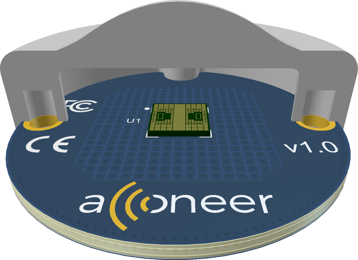
Figure 57 A1 radar sensor with EBGs, dielectric lens and casing.#
Side lobe suppression#
Figure 58 and Figure 59 shows two example EBG array variants. The first variant has EBGs distributed in the E-plane only (Figure 58) whereas second variant have EBG cells covering both E and H-planes.
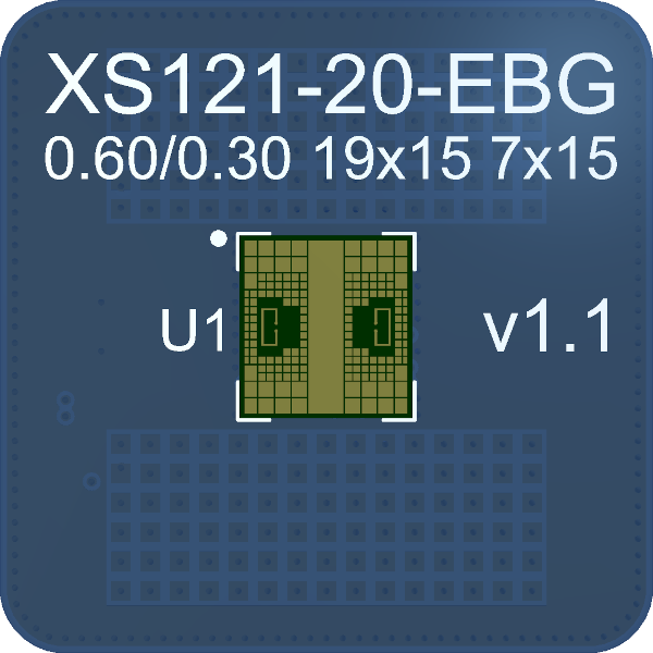
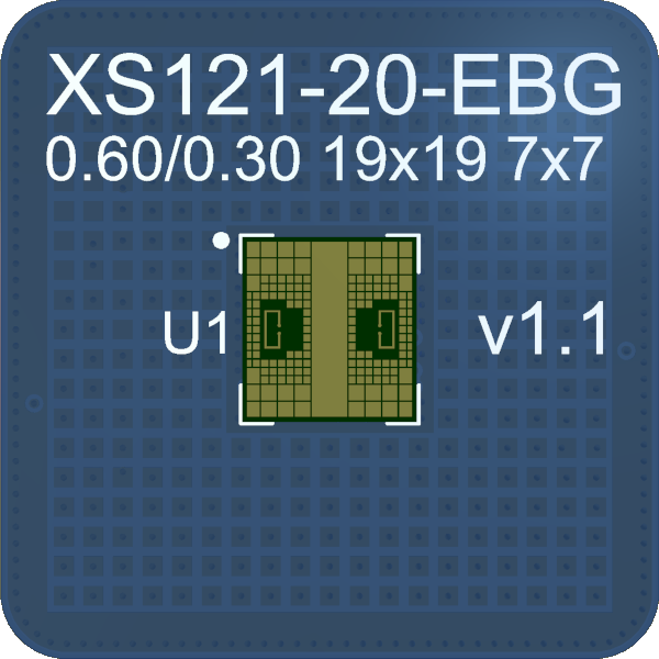
Figure 60 shows Tx+Rx far-field measurements with and without EBGs for two EBG variants. Both variants improve the E-plane side lobe level by approximately 10 dB at +/-90 deg angles. We also notice a small increase in boresight gain as the EBG reflection phase have been optimized. The E and H-plane EBG implementation yields some further SLL improvement with the cost of additional PCB routing complexity.
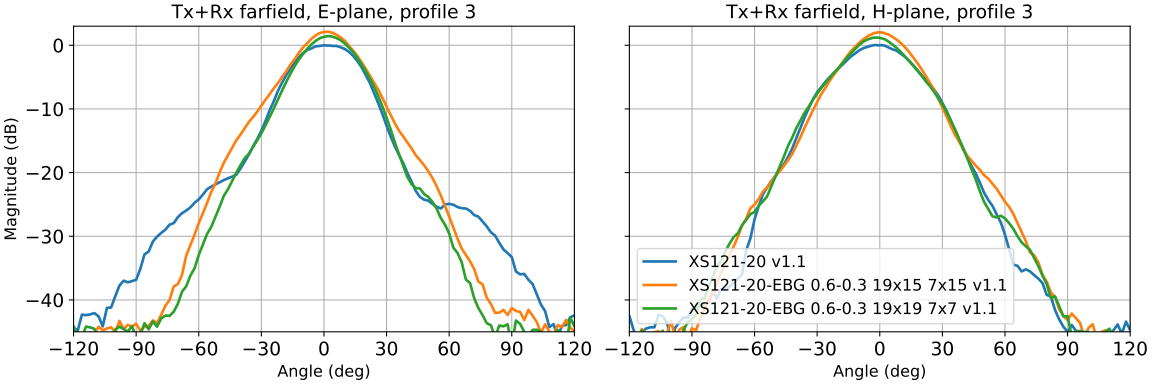
Figure 60 Normalized far-fields with and without EBGs.#
Impact of product enclosure#
Increased side lobes can occur from spillover radiation hitting the product enclosure walls, PCB standoffs and other nearby structures if these need to be close to the sensor (Figure 57). Figure 61 shows how the side lobe level improve with the addition of EBGs, especially in the E-plane. Again, we observe a small increase in boresight gain (~2 dB) with the addition of EBGs.
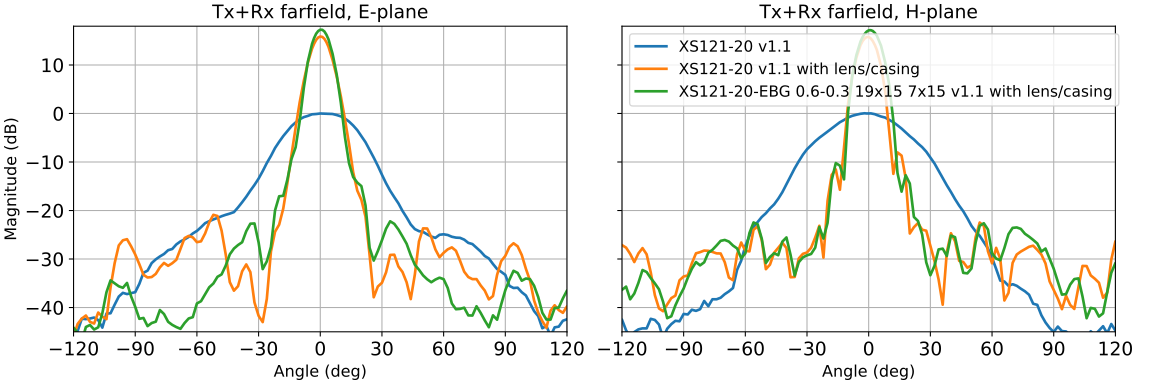
Figure 61 Normalized far-fields with and without EBGs with lens and casing.#
Mushroom type EBGs#
The EBGs used here are mushroom-type EBGs and these are one of the most common and effective structures. A mushroom unit cell consist of a square patch on the top layer with a centered metallic via connected to the ground plane underneath (layer 2), see Figure 62. As multiple EBG cells are formed in an array, we obtain a periodic structure that can manipulate the material properties of the PCB. This allows us to create a spatial filter for suppressing surface currents as well as optimizing the PCB reflection phase.
Both blind vias and through hole vias can be used for constructing the EBG cells. The patch size, element spacing, dielectric thickness and dielectric properties are important tuning parameters for obtaining the desired performance.
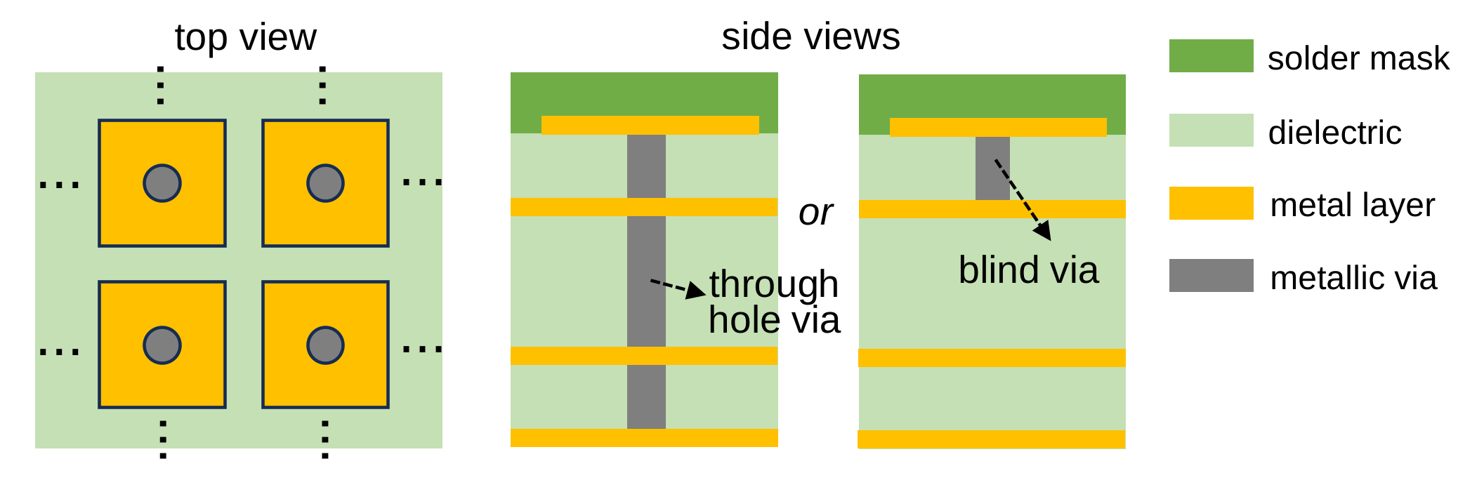
Figure 62 Mushroom-type EBGs.#
PCB guidelines with EBGs#
EBGs for 60 GHz are commonly implemented using RF PCB laminates. However, the EBG variants shown in Figure 58 and Figure 59 are both using FR4 PCB materials to avoid adding material costs. This is possible by tuning the EBG dimensions to allow FR4 material tolerances and choosing specific stackups.
When laying out a PCB, the preferred way is to place all external components such as decoupling capacitors and crystal on the opposite side of the sensor as this typically results in the highest directivity and lowest side lobe level. In addition, to maximize the radiated performance, consider the following:
Layer 2 must be a solid ground plane without routing where the EBGs are applied.
The EBGs have been optimized for 0.20 - 0.25 mm via diameters. This also allows placing signal vias close to the footprint pads.
Minimize the amount of routing on the sensor layer, at least within the clearance region in Figure 36. This can be done by routing the signals to the sensor with vias placed as close as possible to the sensor pads, see Figure 37. The ground plane area inside the footprint has lower impact on the radiated performance and therefore some vias and short traces are preferably placed there.
Whenever the assembly process allows, remove thermal reliefs on all sensor pads.
Minimize copper clearance for traces, vias, and pads on the sensor layer to maximize the ground plane area close to the sensor.
Add stitching vias with <0.6 mm spacing at the PCB outer edge to suppress potential edge radiation.
Contact Acconeer support to obtain more information on EBG implementations.
The exact location and dimensions of the EBG cells are important for optimal performance. When using through-hole vias, signals can be routed between the EBG vias on layer 3 and below, see Figure 63. The E-plane only variant allows more routing area with a small loss in SLL performance. Occasionally, some EBG vias may need to be slightly shifted or removed to fit other signals and components. When this is needed, it is strongly recommended to do this on EBGs farthest away from the sensor as the innermost elements are most important.
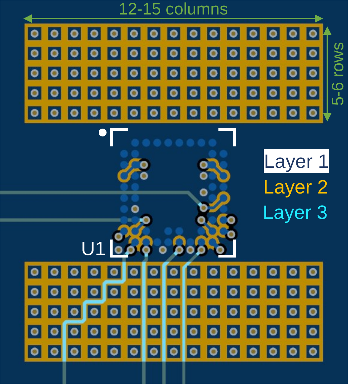
Figure 63 Example mushroom type EBG implementation with routing.#
More information#
EBGs can be implemented using both low-cost FR-4 as well as RF PCBs. To implement EBG structures into your design, please contact the Acconeer customer support for layout recommendations.