
Electromagnetic band-gap (EBG) structures guidelines#
The radar far-field performances can be degraded by side lobes, which represent unintentional sensitivity to directions outside the main beam. In fact, a reflection from a side lobe direction can produce a stronger response than from a weaker target in the main lobe direction. Applications where this typically happens are level sensing in tanks, silos and cargo container measurements where sidewall corners close to the radar with low path loss can produce strong response in comparison to the target object.
At millimeter-wave frequencies, side lobes are often caused by surface currents and surface waves in the PCB. The side lobe level can be significantly improved with the use of horn antennas or reflectors. However, an alternative cost-effective way to improve the side lobe level is by implementing electromagnetic band-gap (EBG) structures.
EBG#
We recommend using EBGs on the PCB to suppress surface waves and surface currents that cause unwanted side lobes and edge effects, therefore preserving the far-field performance. Mushroom-type EBGs are common and effective band-gap structures. Mushroom type EBGs are two-dimensional periodic structures as shown in Figure 56. In each EBG unit, there is a square patch metal layer (always on top of the PCB) connected with a centered metallic via to the ground plane (always a separate layer with PCB routing). Both blind vias and through hole vias can be used to construct the EBG units.
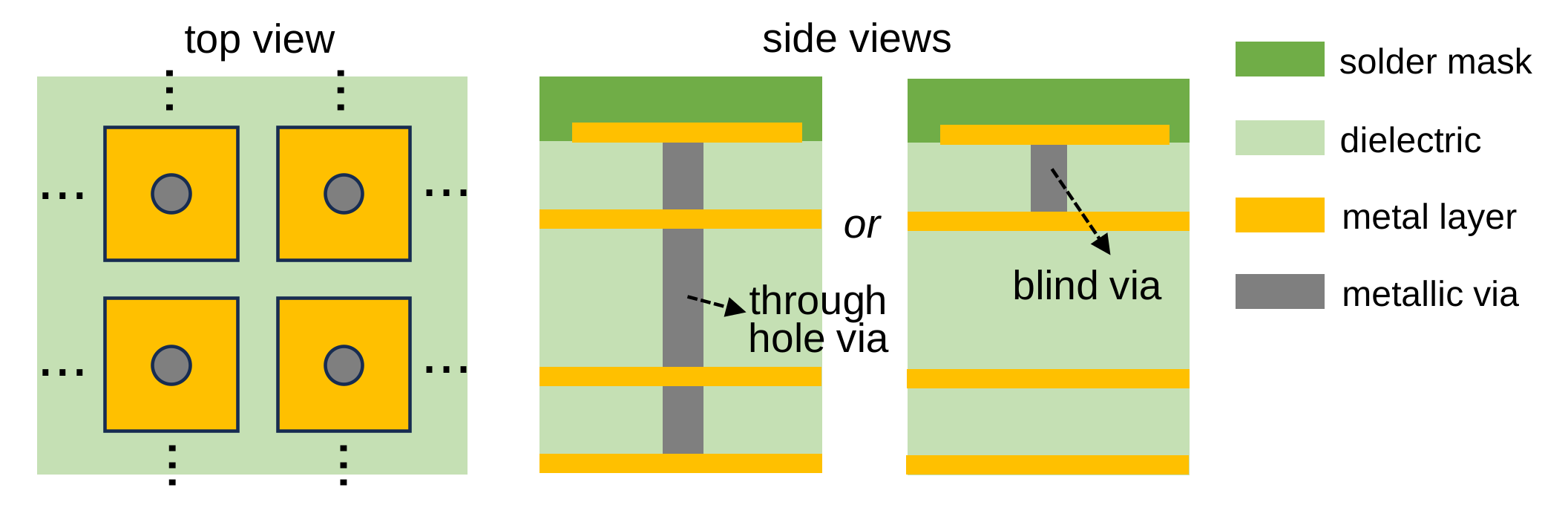
Figure 56 Schematic views of mushroom-type EBGs.#
Figure 57 shows the comparison of the A1 sensor near-field with and without EBG integration on the PCB. The PCB has multiple layers. On the PCB without EBGs, the sensor near-field spreads in all space around and inside the PCB. These fields can cause crosstalk among integrated components. Compared to the PCB with 5-row mushroom EBGs, the sensor near-field is confined within the EBGs, so less fields are spread in space or inside the PCB. Therefore, the far-field radiated from the sensor is well preserved.
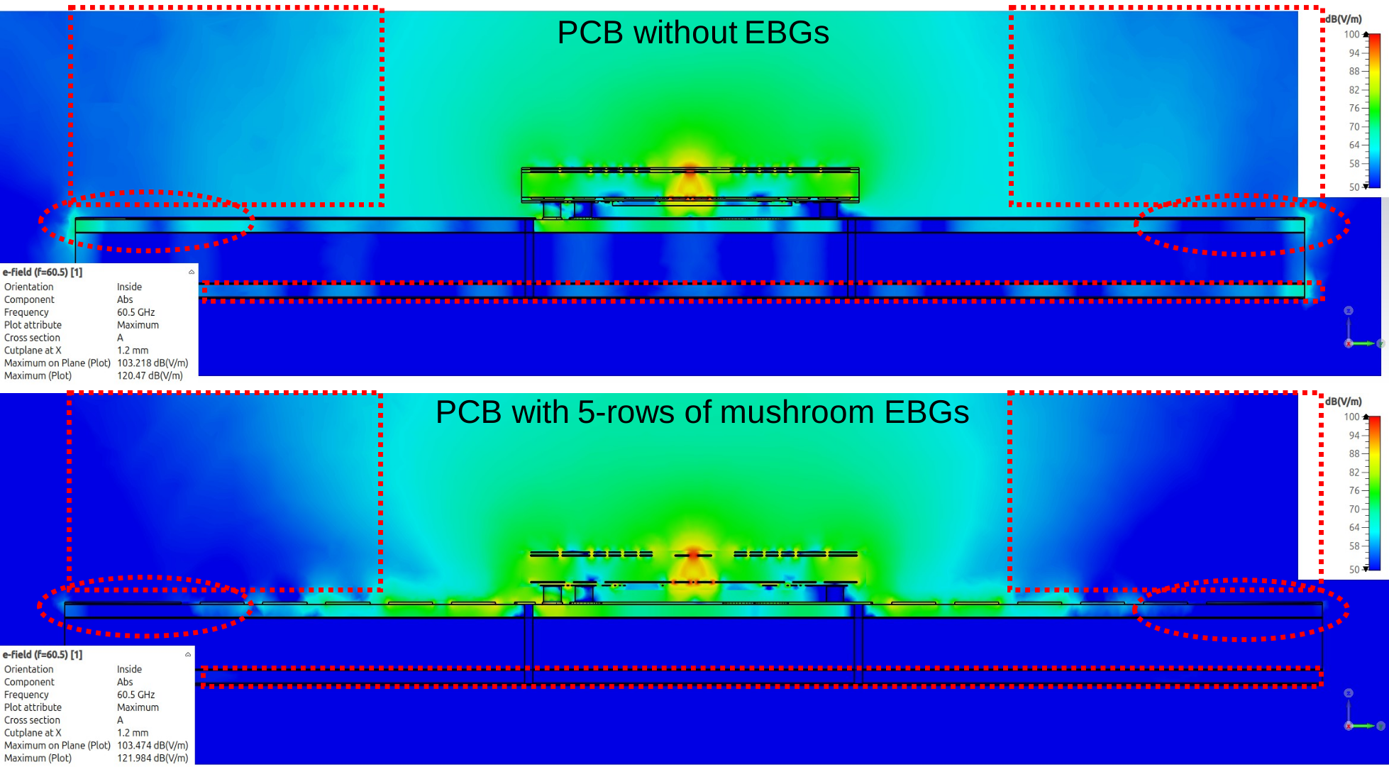
Figure 57 Side views of the electric field distribution for A121 sensor on PCB with and without EBGs.#
PCB routing with EBGs#
The placement of the EBGs with respect to the sensor is important for the best results. EBGs are periodically distributed in horizontal and vertical directions and are always symmetrical on both sides of a plane. As Figure 58 shows, EBGs can be distributed in the E-plane only, which allows more routing area, or distributed in both the E- and H-planes (see PCB guidelines). It is recommended to use at least 5 rows of EBGs in each side next to the sensor.
When using through hole vias for EBGs, we need to zigzag through the vias. In certain regions, EBG vias may need to be removed to avoid short-circuiting component pads on the bottom side. When this is needed, it is strongly recommended to do this on EBGs farther away from the sensor as the innermost EBGs are more important. Layers 1 and 2 should be kept clear from any routing where EBGs are applied. Layer 2 must be a solid ground plane where EBGs are applied. Routing is easier if EBGs can be placed only in the E-plane sides (the left figure).
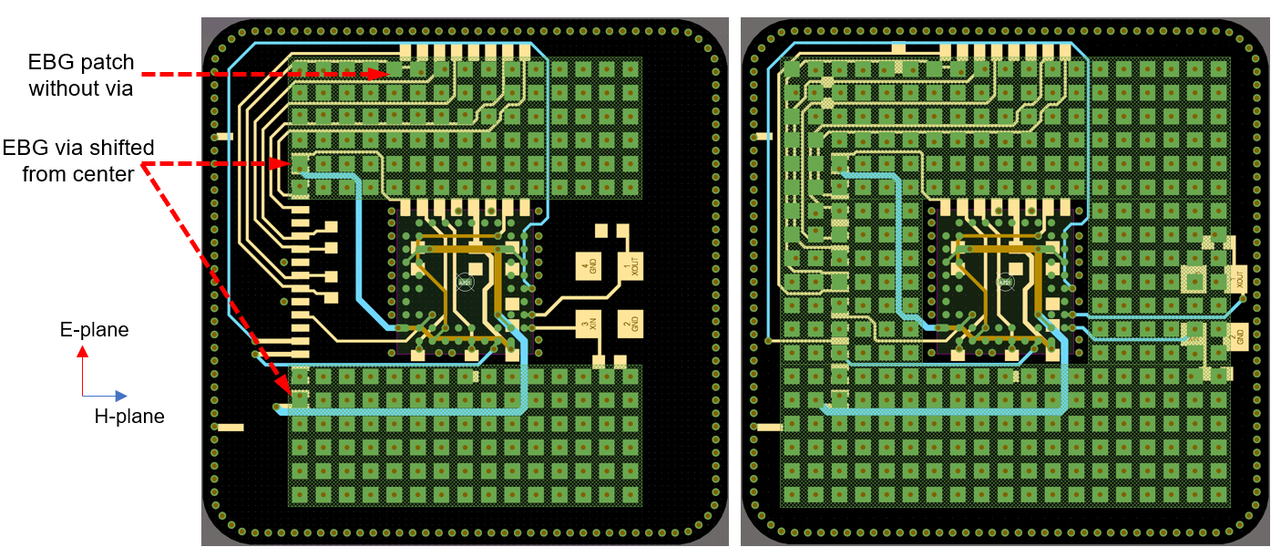
Figure 58 PCB routing example with E-plane EBGs, E- and H-plane EBGs using through hole vias.#
Performance benefits with EBGs#
Figure 59 shows an example of the TX + RX channel far-field performance improvements for A1 sensor on XS121 board with EBGs. Compared to PCB only (no EBG) solution, adding EBGs in the E-plane or both planes can increase the channel beam roll-off rate thus creating a directive channel performance. We also notice an small increase in the far-field boresight gain. Adding EBGs on both the front and back of the PCB can further improve the performance at a cost of occupying more space.
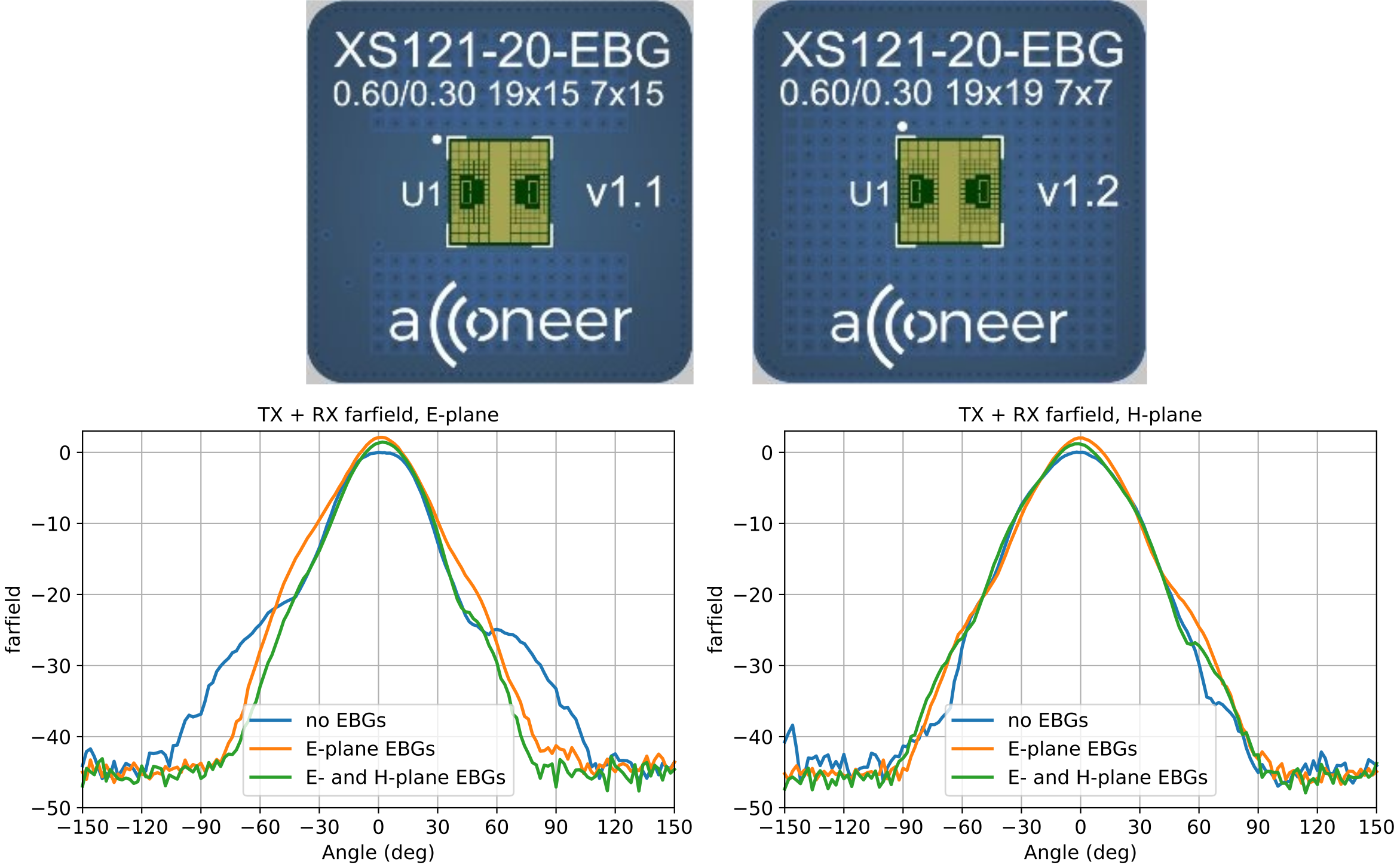
Figure 59 Channel performance comparison (profile 3 excitation) of A121 sensor on PCB and with EBGs.#
The dimensions of the EBG unit (patch + via) and the PCB material (FR-4 or RF materials) define the band-gap frequencies, which should at least cover the radar operating band of 57–64 GHz, so as to suppress the surface waves propagation effectively. Please contact our customer support for more details.