PCB guidelines#
In addition to electrical integration, the electromagnetic environment is important for optimal performance. The A121 pulsed coherent radar sensor is a fully integrated 60 GHz radar sensor with integrated transmitter and receiver antennas. The Tx and Rx antennas are folded-dipole type and the E-plane and H-planes are indicated in Figure 35. The RLG patterns can be found in the A121 Datasheet.
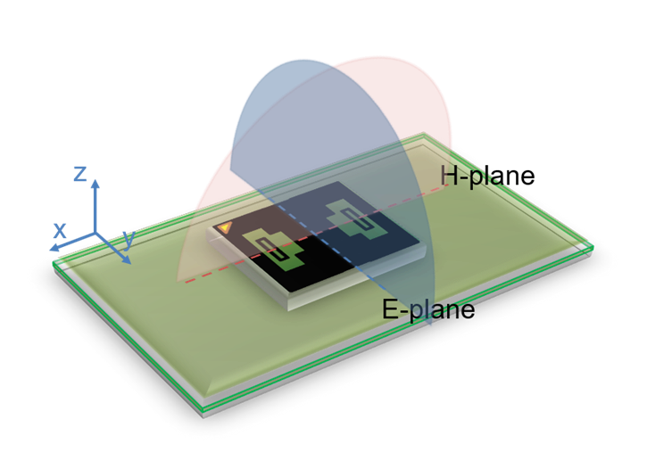
Figure 35 Sensor mounted on a printed circuit board (PCB). E-plane and H-plane are highlighted with blue and red color, respectively.#
Radar loop equation#
Consider a signal transmitted through free space to a radar target located at distance \(R\) from the radar. Assume there are no obstructions between the radar and the radar target, and the signal propagates along a straight line between the two. The channel model associated with this transmission is called a line-of-sight (LOS) channel. For the LOS channel, the corresponding received reflected power from a radar target, i.e. the signal-to-noise ratio (SNR), can be defined as
Where \(R\) is the distance of the radar to the target, \(C\) is the radar loop gain, including both the transmitter and receiver chain (two-ways signal path), \(\sigma\) is the Radar Cross Section (RCS) of the scattering object and \(\gamma\) determines the reflected power of the object’s material. RCS depends on the size and shape of the scattering object. Moreover, SNR depends on the sensor profile setting. A comprehensive explanation of the sensor profiles can be found under section profiles.
Radar loop gain pattern#
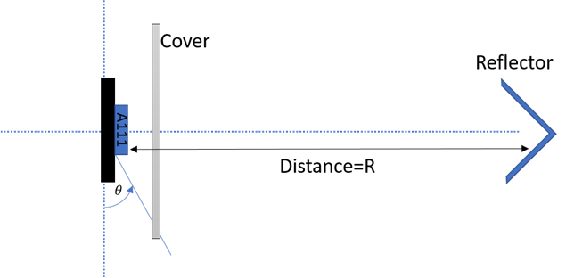
When characterizing the gain, we refer to the radar loop gain defined in the radar equation section. Figure 36 shows the radar setup configuration for the radar loop radiation pattern measurement. The reflector which in this case is a circular trihedral corner is located at the far-field distance from the sensor.
The Sparse IQ service, see Interpreting radar data, can be used to collect the reflected signal at the fixed distance from the radar target for different rotation angles. The figure of merit for amplitude variation stated in the document is the RLG which includes both transmitter and receiver gain of the radar.
PCB Layout#
Sensor ground plane size#
To maximize the RLG and minimize impact on the radiation pattern, it is recommended that the top PCB layer is a filled copper layer with minimum amount of routing close to the sensor. Figure 37 shows the relative loss in RLG as a function of ground plane size, assuming a solid square ground plane and the sensor placed at the center. As the ground plane size is increased, the RLG increases because of increased antenna directivity. However, the RLG does not increase monotonically with ground plane size due to constructive and destructive interference.
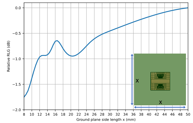
Figure 37 Simulated relative radar loop gain as function of ground plane side length (x). Ground plane is a solid square ground plane without routing.#
In terms of regulatory compliance, any openings in the ground plane inside the A121 BGA footprint must be significantly smaller than the wavelength of the radiation that is being blocked, to effectively approximate an unbroken conducting surface.
Impact of PCB routing and nearby components#
As no RF components are required for the sensor integration, low-cost FR-4 type PCBs can generally be used. However, for a symmetrical RLG pattern and maximum directivity, the following PCB design rules should be considered.
Whenever possible, place decoupling capacitors and the crystal on the opposite side of the PCB. In other cases, the decoupling capacitors can be placed as in Figure 39 and the crystal placed some distance away from the sensor. A small RLG loss of approximately 0.5 dB is seen when placing decoupling capacitors (metric 1005 or smaller), see Figure 41.
Minimize the amount of routing close to the sensor. This can be done by routing the signals to the sensor with vias placed as close as possible to the sensor pads as shown in Figure 38. The ground plane area inside the footprint has lower impact on the radiated performance and therefore some vias and short traces are preferably placed there while still satisfying regulatory compliance.
Minimize copper clearance for traces, vias, and pads on the sensor layer.
If the PCB assembly allows, connect all ground pads without thermal reliefs as shown in Figure 38 and Figure 39. This can increase the boresight RLG by approximately 1.5 dB compared to Figure 40, provided there are no other interfering components or PCB traces close to the sensor, see Figure 41.
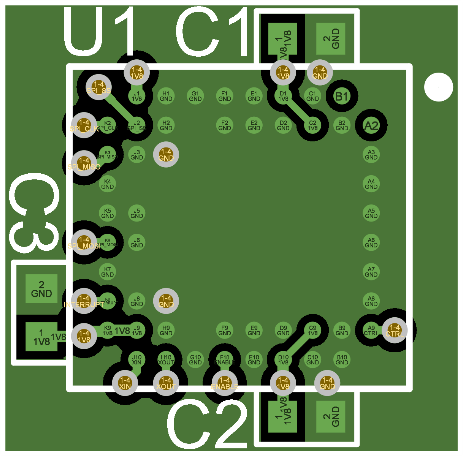
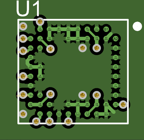

Figure 41 Relative RLG loss with and without thermal reliefs.#
Impact of conformal coating#
Conformal coating may be used to protect the sensor and other electronic components from environmental factors such as moisture, dust, and chemicals. Conformal coatings are typically made of polymeric materials with dielectric constants in the range \(\varepsilon_r\) < 4. Depending on the coating material properties and layer thickness, the sensor’s RLG may decrease. This gain drop is due to three factors:
Offset in antenna resonance frequency as the antenna becomes electrically larger.
Reflection and refraction loss due to the interface between the sensor and the coating.
Dielectric loss in the coating material. This can usually be neglected for this coating layers (e.g. < 200 \(\mathrm{\mu m}\)).
Figure 42 shows the simulated relative RLG after a linear lossless (tan(\(\mathrm{\delta}\)) = 0) isotropic coating has been added to all sides of the radar sensor. As the coating thickness increases and/or the dielectric constant increases, the RLG decreases. However, this loss is non-monotonic, and this is due to constructive and destructive interference depending on the coating thickness.
The loss due to antenna resonance frequency offset can be seen in Figure 43 and Figure 44 where the maximum gain is shifted in frequency. This means that, as the radar signal is a wideband signal, the resulting loss in SNR can be expected to be somewhat less than what is estimated in those.
If it is critical to obtain the maximum gain, it is recommended to use a thin coating layer (< 40 \(\mathrm{\mu m}\)) with a low dielectric constant and loss factor. As many coating materials are not well characterized at mmWave frequencies. performance should be verified with actual tests.

Figure 42 Simulated impact of lossless dielectric conformal coating on RLG at 60 GHz.#


For more information, see:
Hardware integration guideline, in section Electromagnetic Integration