Lens design#
Dielectric lenses are a cost-effective way of shaping the radiation patterns, especially for mmWave applications where the size of the lens becomes small enough. Although it is most common to design lenses for increasing the gain and to narrow the beamwidth, lenses can also be used for increasing the beamwidth, produce tilted beams, or suppress side lobes to reject unwanted reflections.
Since many common thermoplastics used in the product design also have low permittivity and low loss, a lens can often be incorporated into the same encapsulation material with little additional cost. 3D printing technology allows for rapid prototyping and can often resemble the performance of the final product. Dielectric lenses are generally more compact and less expensive to fabricate than corresponding horn antennas and reflectors.
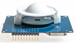
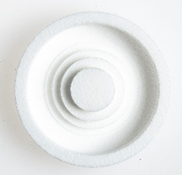
To quickly get started using a lens, Acconeer provides two example lenses, one plano-convex and one FZP type lens, Figure 45 and Figure 46. Both lenses can be used with all module evaluation kits. The FZP lens is similar to the example lens in Example FZP lens calculation. The user guide and performance of these lenses can be found in A121 Lenses Getting Started Guide.
Refracting lenses#
Design Principles#
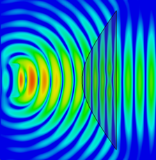
Figure 47 shows a spherical wavefront from the A121 sensor feeding a converging lens of refractive index \(n = \sqrt{\varepsilon_r}\). The lens refracts the spherical waves to produce parallel waves for increasing the directivity. Figure 48 shows the corresponding ray optics model where rays propagate from the source as diverging straight lines until hitting the first surface and refracting into parallel rays. Ray optics does not account for interference, diffraction, and polarization but it provides a basic understanding of dielectric lenses, and most importantly, allows us to quickly construct analytical lens shapes for many applications.
In the following we assume that all lens profiles are axisymmetric, although asymmetrical lenses can be designed for customized radiation patterns. For a converging lens, two criteria need to be fulfilled:
Refraction at one or both surfaces to produce parallel rays at the output.
The rays just outside the outer surface have to be coherent (in-phase).
One of the lens surfaces can be chosen arbitrarily, for example planar or spherical. Next, we will provide design equations for constructing converging lenses fulfilling these criteria.

Convex-planar lens (Hyperboloidal lens)#
By constraining the outer surface to planar we have \(x_{2} = F + T\), Figure 48. Equating the optical path through a point (\(x_{1},y_{1}\)) with the central path yields
Eq. 18 can be written as
where the coefficients are given by
Observe that we have refraction only at the inner surface, that is, this is a single refracting lens. We recognize Eq. 20 as a hyperbolic function shifted in the \(x\) direction by \(x_{0}\), hence the name hyperbolic (2D) or hyperboloidal (3D) lens.
The central thickness of the lens can be shown to be
To generate a lens profile, we first choose a material \(n = \sqrt{\varepsilon_r}\). After this the diameter \(D\) and the focal distance \(F\) is chosen to fulfill some maximum thickness requirement in Eq. 21. The lens profile is then given by Eq. 19 by solving for \(y_{1} = y_{1}(x_{1}), x_{1}\in [F, F+T]\). A parametrization \((x_{1}(t),y_{1}(t))\) may be required for generating the lens profile in CAD software. One such parametrization is
Plano-convex lens#
Constraining the inner surface to planar results in a plano-convex lens, see Figure 49. We then have \(x_{1} = F\) and carrying out the algebra results in the following parametric solution for the outer surface:

Figure 49 Plano-convex lens ray model.#
The central thickness is given by
Contrary to the hyperboloidal lens, we now have refraction at both the inner and the outer surfaces. The lens profile given in Eq. 23 do not resemble any known function and we therefore simply call this lens a plano-convex lens.
Lens gain#
The lens gain is related to the lens effective area by \(G = \frac{4 \pi A_{e}}{\lambda^{2}}\) where \(\lambda\) is the wavelength in the dielectric material. Approximating the effective area with the lens inner surface area \(A_{e} = \pi \left(\frac{D}{2}\right)^{2}\), we obtain \(G = \left(\frac{\pi D}{\lambda}\right)^{2}\). We thus notice that the lens gain is proportional to the square of the diameter. To get the lens RLG, we double the lens gain, because of the Tx and Rx path.
Figure 50 and Figure 51 show simulated RLG pattern plots for the hyperbolic and the plano-convex lenses for some sample values of F and D. These figures can be used as a rough guideline for choosing the lens size. Observe that for the same diameter, the plano-convex lens yields somewhat higher gain compared to the hyperbolic lens. The exact RLG pattern will also depend on the lens housing, choice of material, and PCB size.

Figure 50 Simulated RLG patterns for different size hyperbolic lenses assuming lossless dielectrics.#

Figure 51 Simulated RLG patterns for different size plano-convex lenses assuming lossless dielectrics.#
Fresnel Zone Plate (FZP) lenses#
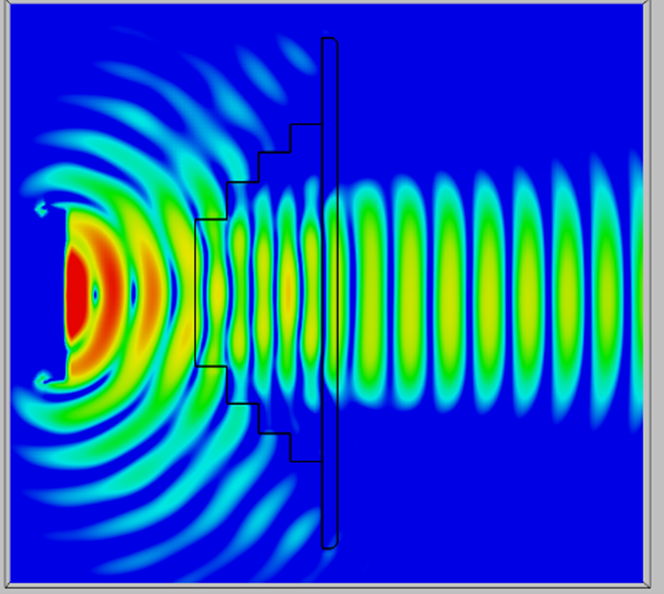
The plano-convex and convex-planar type lenses are refracting type lenses. Another popular lens type is the Fresnel zone plate lens which is based on diffraction instead of refraction. Different types of FZP lenses exists and here the phase correcting FZP lens is covered. The FZP lens structure is composed of dielectric rings with different thickness for correcting the phase of the incident waves. Figure 52 shows an example of FZP lens consisting of 3 zones with the phase step of quarter of a wavelength.
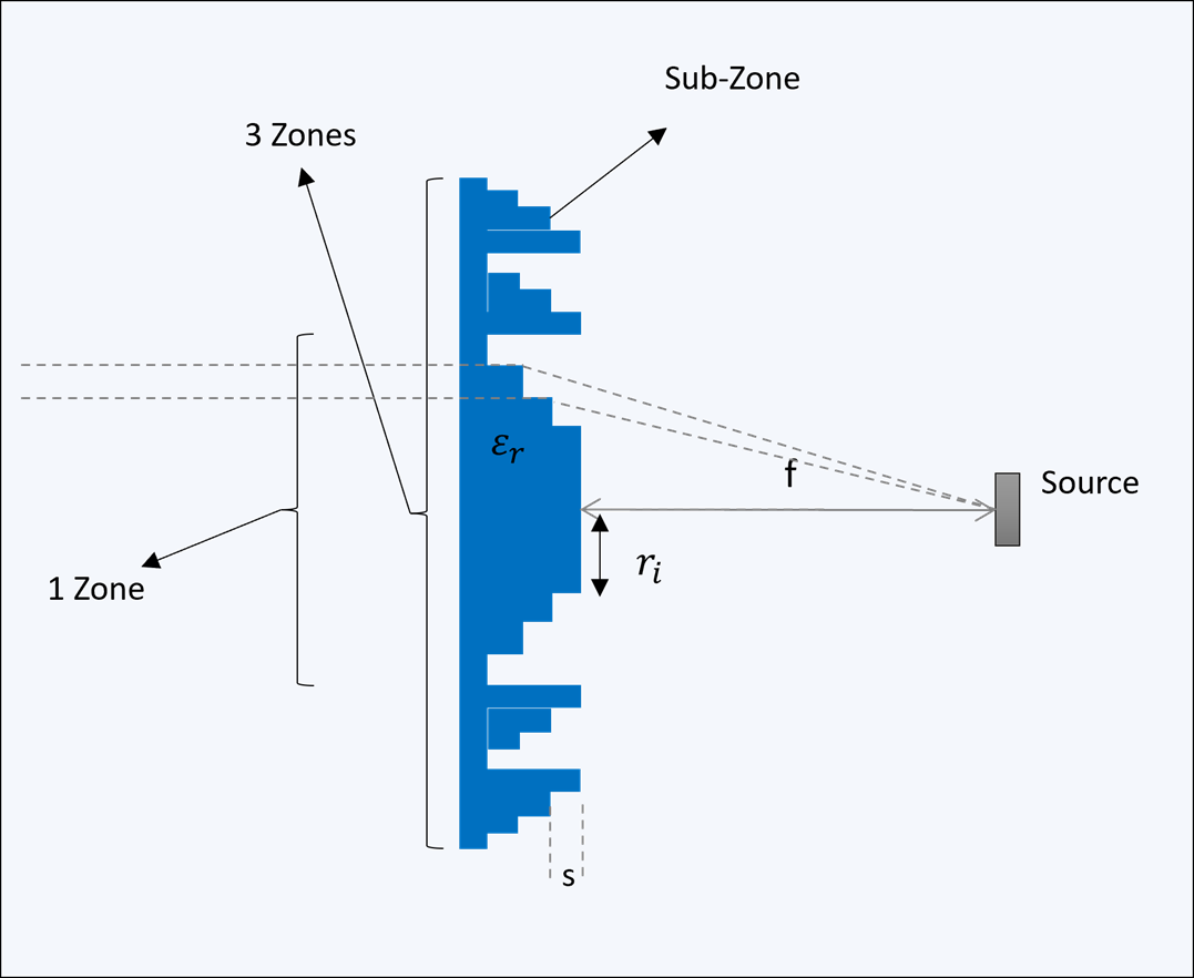
The radius \(r_{i}\) of the rings and the step thickness \(s\) can be calculated with:
Here \(F\) is the focal point, \(P\) is the number of sub-zones, or steps, \(\lambda_{0}\) is the wavelength in free space ( 5 mm at 60 GHz), and \(\varepsilon_r\), is the relative dielectric constant. For small diameter lenses, we can choose one zone and 4 or 8 steps. For larger diameter lenses, additional sub-zones can be added for increased gain. Notice that contrary to the refracting type lenses, the ring thickness and hence the total thickness is independent of the lens radius. This allows us to construct large diameter lenses without increasing the thickness.
Example FZP lens calculation#
This is an example of a single zone FZP lens with a focal point F = 10 mm and quarter of wavelength step, N = 4. We assume material permittivity of \(\varepsilon_r\) = 2.6. Inserting this into Eq. 25 gives us the lens radii as follows:
\(r_{1}\) = 5.1 mm
\(r_{2}\) = 7.46 mm
\(r_{3}\) = 9.39 mm
\(r_{4}\) = 11.12 mm
Eq. 26 gives us the step thickness of s = 2.02 mm. Total thickness of the lens is then 4*2.02 = 8.1 mm.
For further details regarding FZP lens design, see [1].
Lens thickness comparison#
For mass production, injection molding is usually cost effective but producing thick lenses can be challenging as sink marks and other deformations can occur. It is therefore of interest to find lens designs which are as thin as possible. In Figure 54 we have compared the lens thickness to diameter ratio (T/D) as a function of \(\varepsilon_r\). Common thermoplastics have \(\varepsilon_r\) in the range 2-4 and the hyperboloidal lens is the thinnest lens. To obtain even thinner lenses, the F/D ratio can be increased; however, this may also increase side lobe levels due to spillover radiation, especially for small-diameter lenses.

Figure 54 Lens thickness comparison.#
Lens design guidelines and prototyping#
In general, multiple design aspects must be considered when choosing a lens type. Whenever possible, the lens can be made as a part of the outer enclosure and therefore avoid the need for an additional radome. For applications requiring a flat outer surface, convex-planar or FZP lenses are good choices. Outdoor applications may need to consider rain or ice buildup and here the lens outer surface is chosen to minimize this impact. For example, an upwards pointing convex surface would collect less rain.
Manufacturing lenses by injection molding may pose limitations on the lens maximum thickness. For the refracting type lenses, thin lenses are obtained by choosing a high F/D ratio and higher permittivity materials. On the other hand, higher F/D ratios occupy more space as well as increased spillover energy which in turn leads to larger side lobes. For the plano-convex and convex-planar lenses, it is therefore recommended to keep 0.3 < F/D < 0.6. Lens design with F/D outside this range is certainly possible, but with additional loss in directivity and increased side lobes. When large diameter lenses are required, FZP type lenses should be considered as it’s thickness only depends on the permittivity and are thus generally thinner than refracting type lenses.
For maximum gain and low side-lobe levels, it is important to also follow the PCB ground plane guidelines in Sensor ground plane size.
Focal distance tuning#
The focal distance \(F\) is an input parameter for all lens designs provided here. However, the optimal focal distance may need to be slightly adjusted such that the reflection from the lens is simultaneously minimized. In addition, other effects can impact the focal point, such as material permittivity being slightly off, impact of lens housing, radomes and other nearby mechanics.
Figure 55 shows the gain variation of the integrated lens with the radome with respect to the free space scenario for the XM112 module. The maximum gain happens at 7.5 mm distance for both lenses. Other maxima happen every half-a-wavelength (2.5 mm).
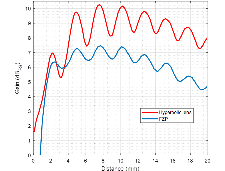
Figure 55 Gain variation of the lens versus the distance to the XM112 radome. The amplitude is normalized to free space (FS). Gain is stated in one direction (Tx or Rx side). For RLG the values will be doubled.#
Customized lenses#
The lens design equations provided here are based on ray optics and may not be adequate in more challenging applications, especially when the lens diameter is small. With a full wave EM solver, Acconeer can construct optimized lenses for maximizing the gain, minimizing the side lobes or customizing the radiation pattern. The impact of lens housings, nearby mechanics and the PCB can also be simulated. Acconeer provides a design service for this, visit the Acconeer Developer page for details.
For more information, see:
Footnotes